Advanced solder materials for high temperature application-their nature, design, process and control in a multiscale domain
| Project start: | 01.05.2007 |
|---|
| Project end: | 30.04.2011 |
|---|
| Programme: | COST |
|---|
| Project number: | COST Action MP 0602 |
|---|
| Institute position in the project: | Partner |
|---|
| Project leader at the institute: | Pavol Šebo |
|---|
The main objective of the project was the study of properties of advanced solder materials for high temperature application for electronics. The main part is directed for joining heat sink material with cooling system in the divertor of fusion reactor. Influence of antimony and copper in lead-free solder Sn-Sb-Cu on the melting and solidification temperatures and on the microstructure of the interface between solder and copper substrate was studied. Melting and solidification temperatures of solder as well as transition zone at the interface between solder and copper substrate were stated. The zone was created by diffusion reaction making Cu3Sn and Cu6Sn3 phases.
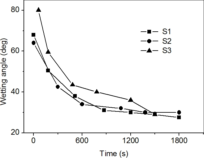
Time dependences of the wetting angle of Sn-Sb solders with various Sb content (Sn-5Sb (S1), Sn-10Sb (S2) and Sn-20 Sb (S3)) on copper substrate during 1800 s at 623 K in N
2+10%H
2 atmosphere.