Services / Material structure characterization /
The TEM operates on the same basic principles as the light microscope but uses electrons instead of light. Because the wavelength of electrons is much smaller than that of light, the optimal resolution attainable for TEM images is many orders of magnitude better than that from a light microscope. Thus, TEMs can reveal the finest details of internal structure - in some cases as small as individual atoms.The beam of electrons from the electron gun is focused into a small, thin, coherent beam by the use of the condenser lens. The beam then strikes the specimen and parts of it are transmitted depending upon the thickness and electron transparency of the specimen. This transmitted portion is focused by the objective lens into an image on phosphor screen or charge coupled device (CCD) camera. The image then passed down the column through the intermediate and projector lenses, is enlarged all the way.
Scanning transmission electron microscopy (STEM) combines the principles of transmission electron microscopy and scanning electron microscopy and can be performed on either type of instrument. STEM also requires very thin samples and looks primarily at beam electrons transmitted by the sample. Principal advantages over TEM is in enabling the use of other of signals that cannot be spatially correlated in TEM, including secondary electrons, scattered beam electrons, characteristic X-rays, and electron energy loss.The STEM technique scans a very finely focused beam of electrons across the sample in a raster pattern. Interactions between the beam electrons and sample atoms generate a serial signal stream, which is correlated with beam position to build a virtual image. Its primary advantage over conventional SEM imaging is the improvement in spatial resolution.
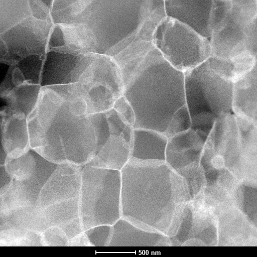 STEM dark-field figure of the microstructure
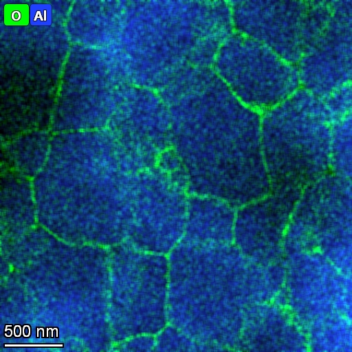 Coresponding EDX map of Al, O elements
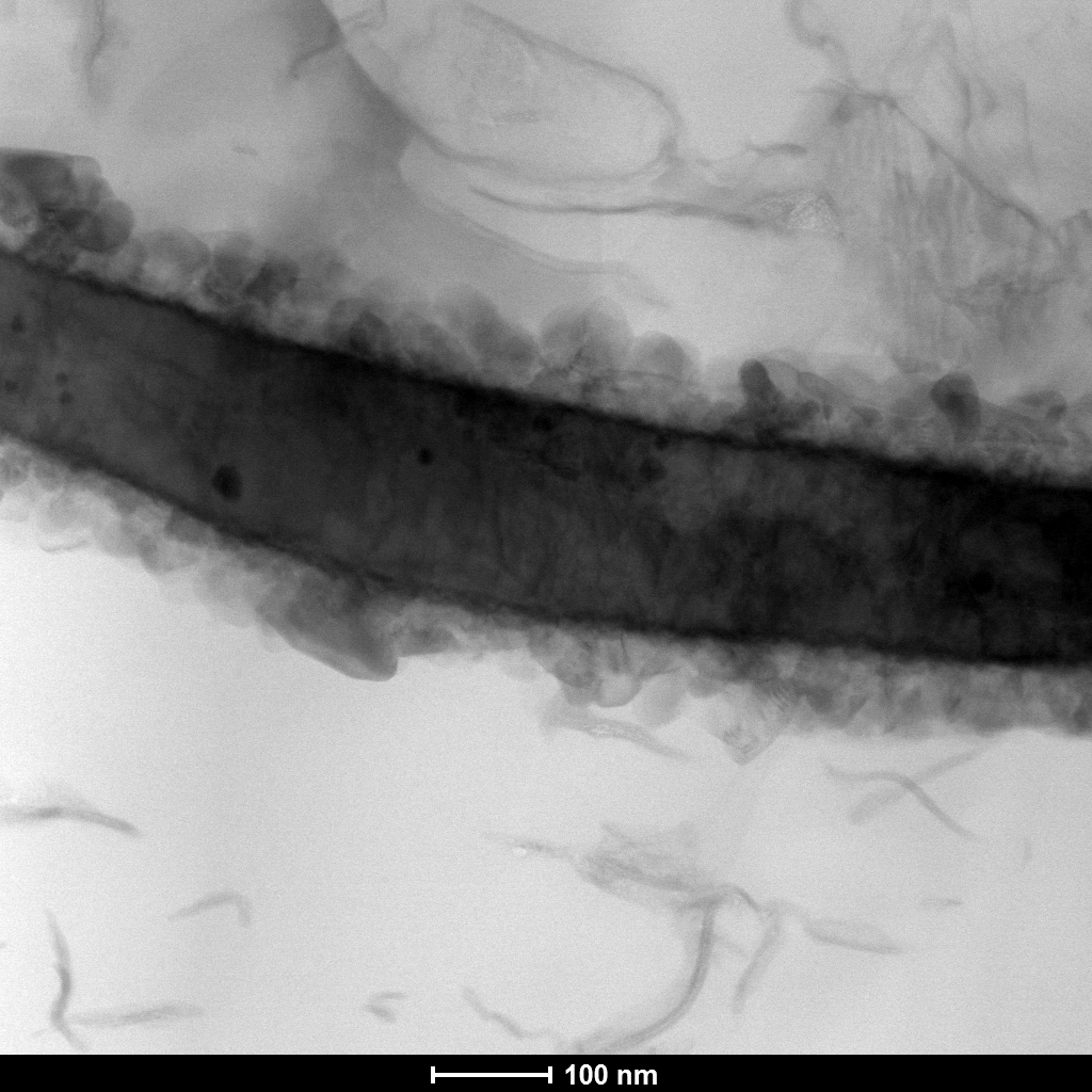
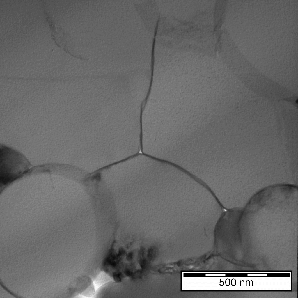 TEM bright-field indicating triple point powder interface with continius oxide
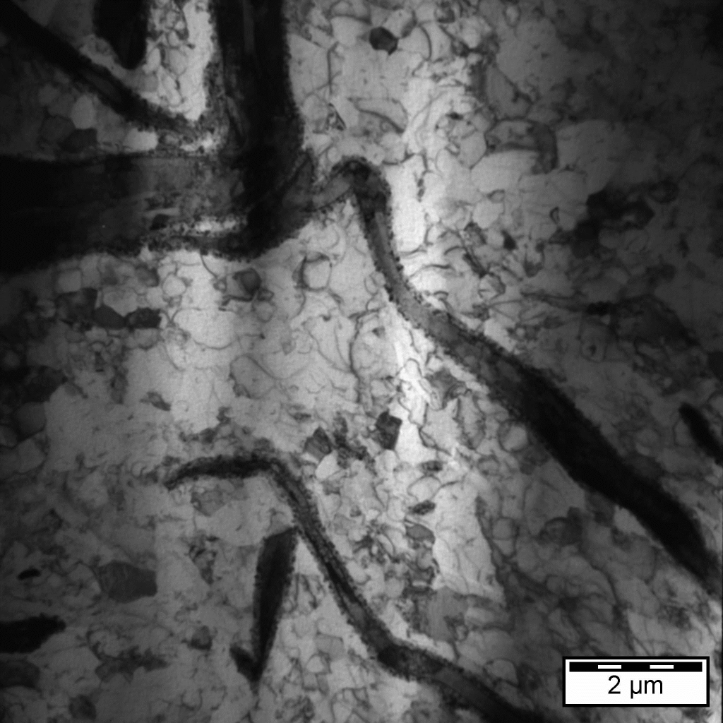
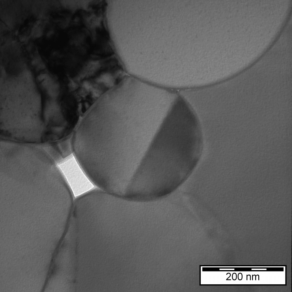 TEM bright-field showing aluminum powder with low angle interface
 TEM bright-field microstructure of Al/Ti composite
 STEM bright-field detail of elongated Ti phase
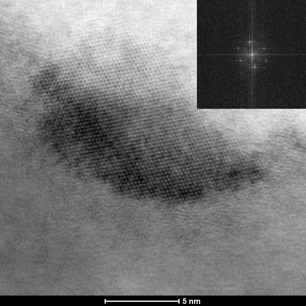 STEM atomic resolution of Al3Ti phase on the interface
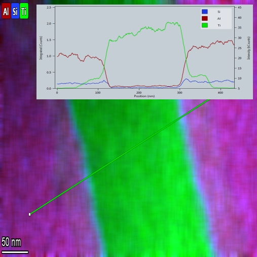 EDS map of Al, Si, Ti elements with line scan measurement
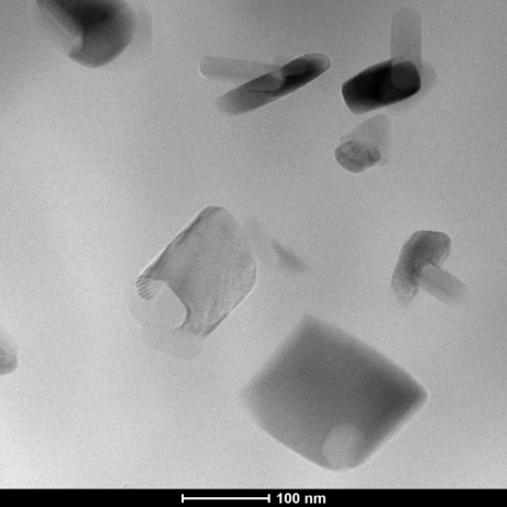 STEM microstructure of precipitates
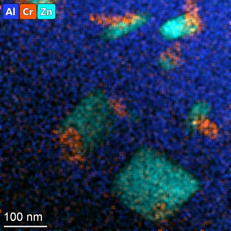 Corresponding EDS map
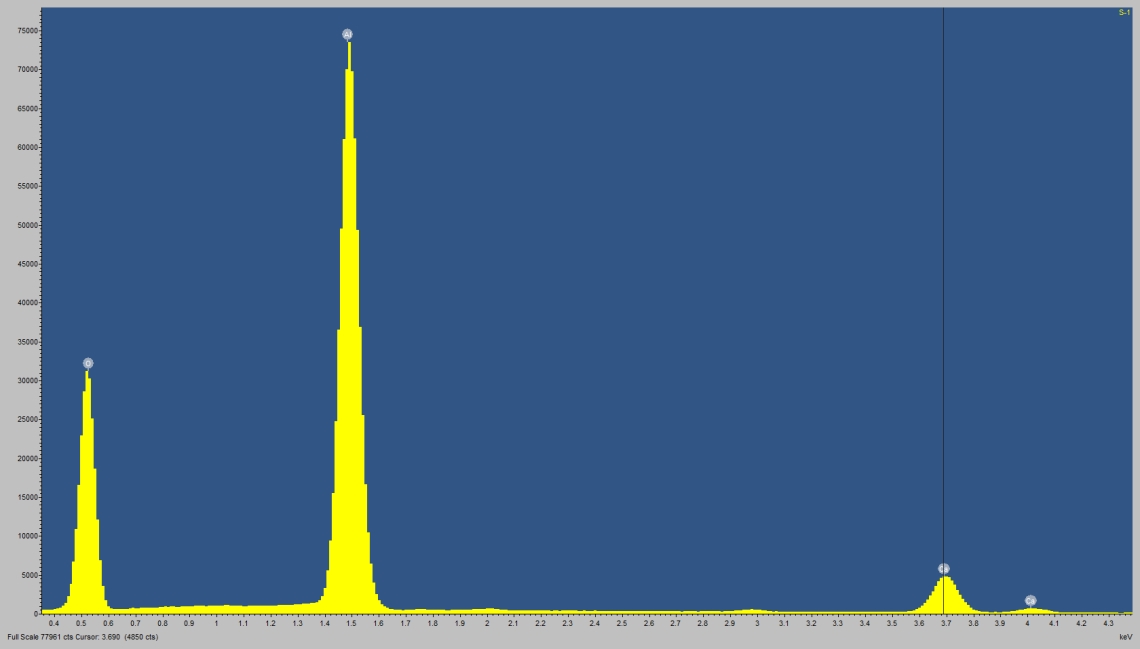
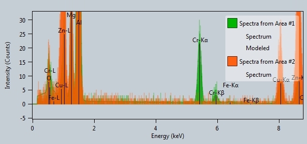 EDS energy spectrum for different precipitates
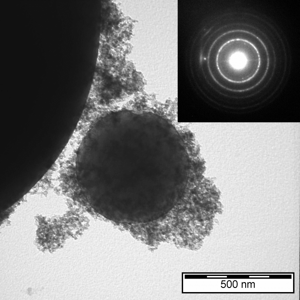
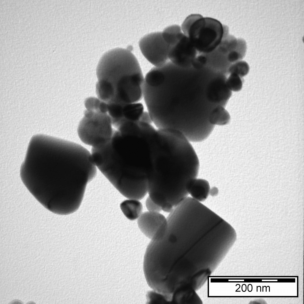 Nanoparticles of ZrO2
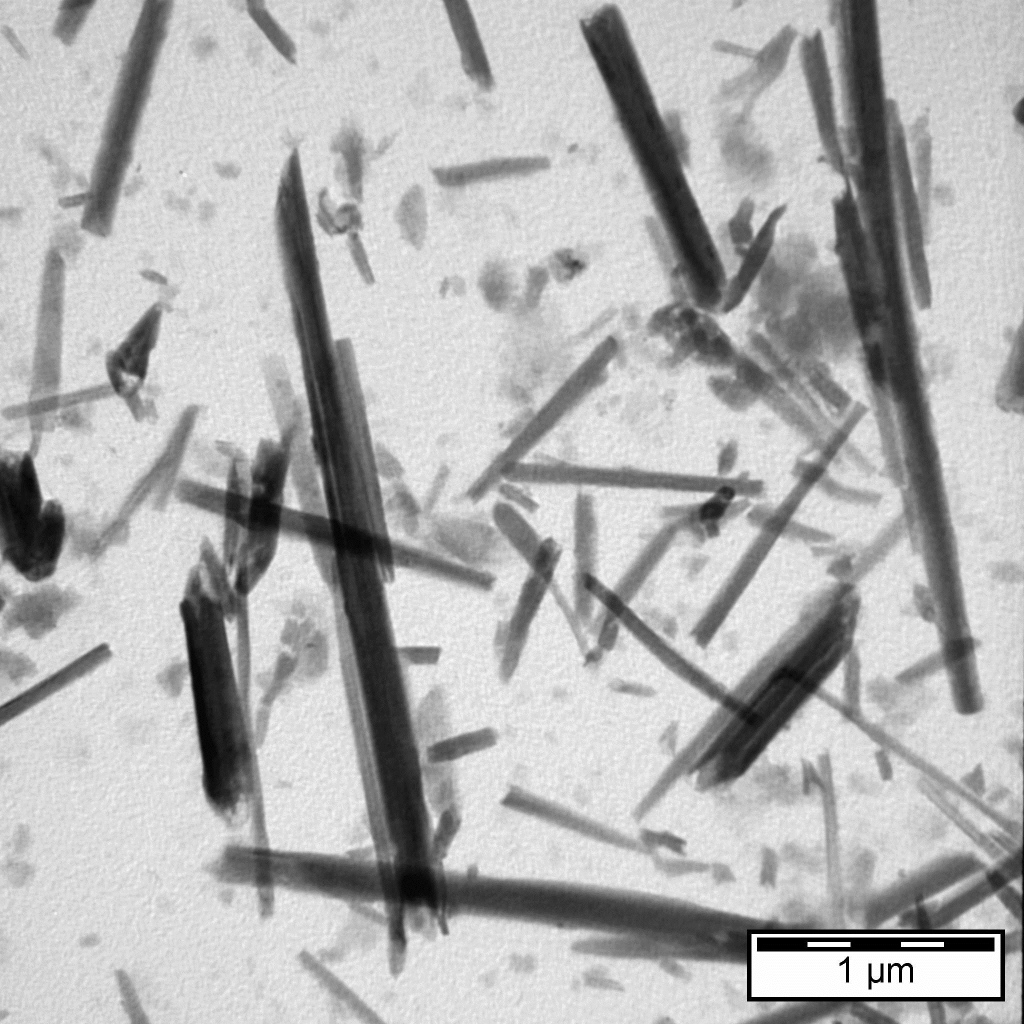 Nanotubes of halloysite
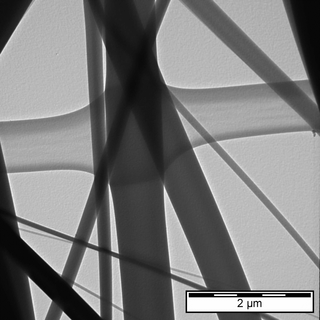 Silk microfibers
 Characterization of natural oxide on the surface of Mg powders
In most applications, data are collected over a selected area of the surface of the sample, and a 2-dimensional image is generated that displays spatial variations in these properties. Areas ranging from approximately 1 cm to 5 microns in width can be imaged in a scanning mode using conventional SEM techniques (magnification ranging from 20X to approximately 30,000X, spatial resolution of 50 to 100 nm). The SEM is also capable of performing analyses of selected point locations on the sample; this approach is especially useful in qualitatively or semi-quantitatively determining chemical compositions using energy disperssive X-ray spectroscopy (EDS) or wave dispersive X-ray spectroscopy (WDS), crystalline structure, and crystal orientations using electron backscattered diffraction (EBSD).
Secondary electrons and backscattered electrons are commonly used for imaging samples: secondary electrons are most valuable for showing morphology and topography on samples and backscattered electrons are most valuable for illustrating contrasts in composition in multiphase samples (i.e. for rapid phase discrimination).
X-ray generation is produced by inelastic collisions of the incident electrons with electrons in discrete orbitals (shells) of atoms in the sample. As the excited electrons return to lower energy states, they yield X-rays that are of a fixed wavelength (that is related to the difference in energy levels of electrons in different shells for a given element). Thus, characteristic X-rays are produced for each element in a mineral that is "excited" by the electron beam. SEM analysis is considered to be "non-destructive"; that is, x-rays generated by electron interactions do not lead to volume loss of the sample, so it is possible to analyze the same materials repeatedly.
Backscattered electron images (BSE) can be used for rapid discrimination of phases in multiphase samples. SEMs equipped with diffracted backscattered electron detectors (EBSD) can be used to examine microfabric and crystallographic orientation in many materials.
 Macro
Macro
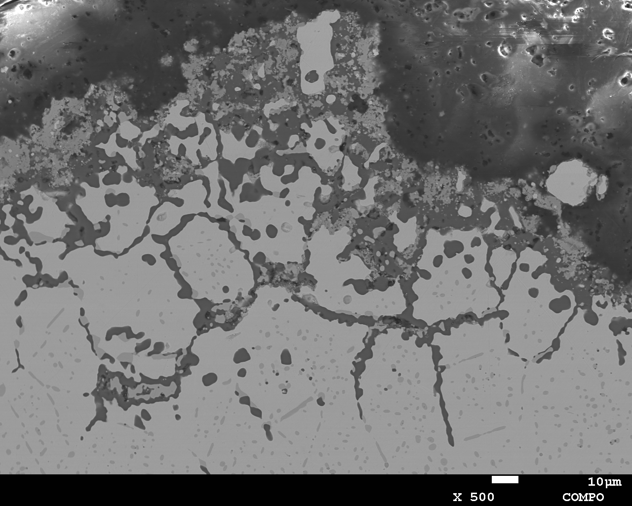 COMPO
COMPO
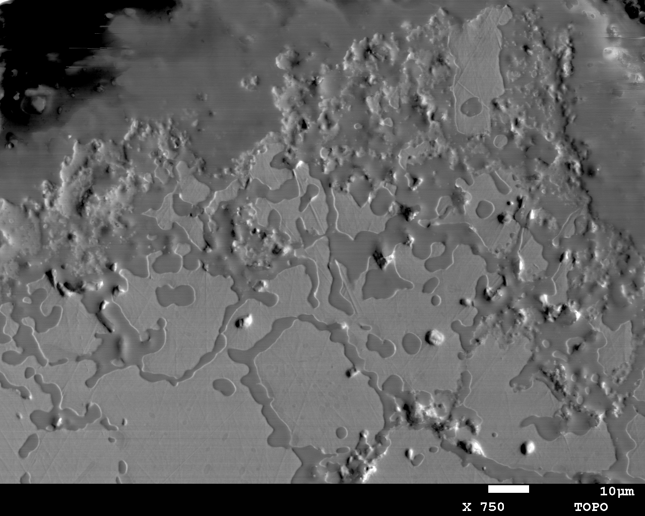 TOPO
TOPO
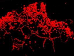
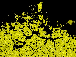
EDS mapping revealing the distribution of selected elements in the corroded structure of the sintering belt
 O Ka1
O Ka1
 Fe Ka1
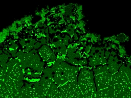 Cr Ka1
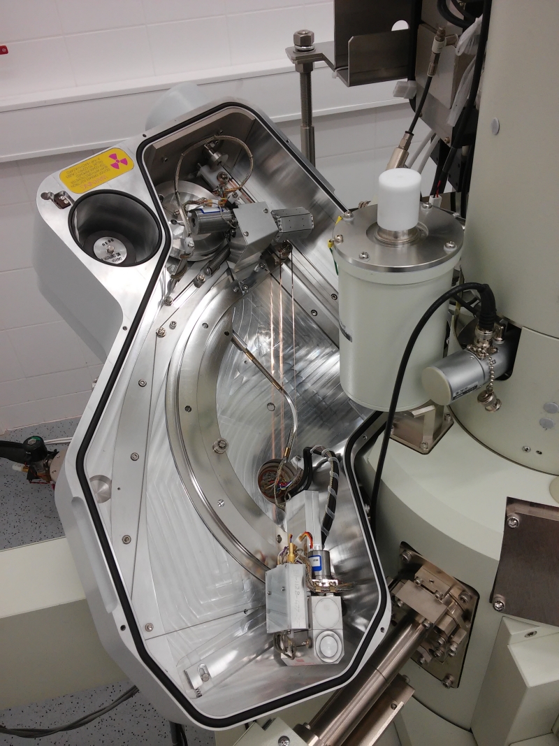 Inner view of WDS detector
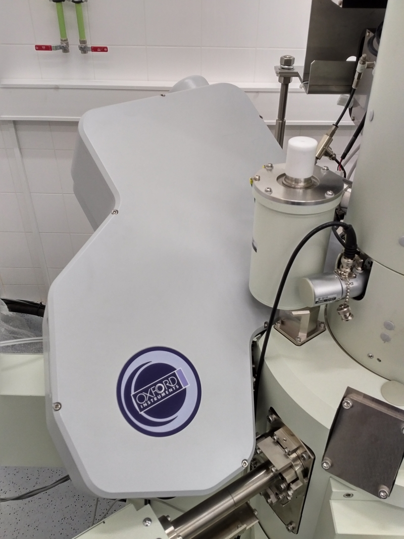 Outer view of WDS detector
Due to increased sensitivity of the WDS, the technique is mainly used to: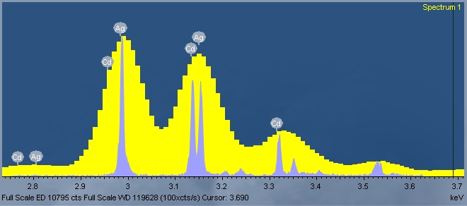
 Schematic description of the characteristic X-ray formation
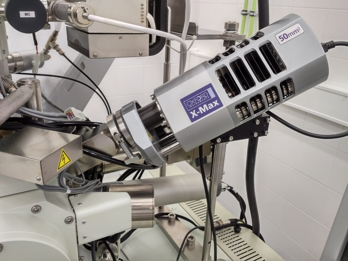 EDS detector
Microstructural analysis
Transmission electron microscopy
General purpose
Transmission electron microscopy (TEM) is a microscopy technique of characterizing materials down to the atomic limits. The beam of electrons is transmitted through an ultra-thin specimen, interacting with the specimen as it passes through it. The TEM generates a tremendous range of signals so we can obtain atomic-resolution images of materials and their defects, together with spectroscopic data and diffraction patterns from sub-nanometer regions. TEMs have a wide-range of applications and can be utilized in a variety of different scientific, educational and industrial fields. TEM offer the most powerful magnification, potentially over one million times or more.Principle of operation
A TEM specimen must be thin enough to transmit sufficient electrons to form an image with minimum energy loss. For most materials, a common sequence of preparation techniques is mechanical thinning, dimpling, and ion-milling.The TEM operates on the same basic principles as the light microscope but uses electrons instead of light. Because the wavelength of electrons is much smaller than that of light, the optimal resolution attainable for TEM images is many orders of magnitude better than that from a light microscope. Thus, TEMs can reveal the finest details of internal structure - in some cases as small as individual atoms.The beam of electrons from the electron gun is focused into a small, thin, coherent beam by the use of the condenser lens. The beam then strikes the specimen and parts of it are transmitted depending upon the thickness and electron transparency of the specimen. This transmitted portion is focused by the objective lens into an image on phosphor screen or charge coupled device (CCD) camera. The image then passed down the column through the intermediate and projector lenses, is enlarged all the way.
Scanning transmission electron microscopy (STEM) combines the principles of transmission electron microscopy and scanning electron microscopy and can be performed on either type of instrument. STEM also requires very thin samples and looks primarily at beam electrons transmitted by the sample. Principal advantages over TEM is in enabling the use of other of signals that cannot be spatially correlated in TEM, including secondary electrons, scattered beam electrons, characteristic X-rays, and electron energy loss.The STEM technique scans a very finely focused beam of electrons across the sample in a raster pattern. Interactions between the beam electrons and sample atoms generate a serial signal stream, which is correlated with beam position to build a virtual image. Its primary advantage over conventional SEM imaging is the improvement in spatial resolution.
Application of the technique
A transmission electron microscope is ideal for a number of different fields such as life sciences, nanotechnology, metallurgy, medical, biological, and material research. TEMs provide topographical, morphological, compositional and crystalline information.The images allow researchers to view samples on a nanostructural level, making it possible to analyze structure and texture. This information is useful in the study of crystals and metals, but also has industrial applications. The transmission electron microscope (TEM) has emerged as the perfect tool for out exactly what new material we have made, and how perfect it is. It can now give us atomic-resolution images of materials and their defects, together with spectroscopic data and diffraction patterns from sub-nanometer regions.Typical case studies
PM aluminium microstructure characterisation
STEM dark-field figure of the microstructureCoresponding EDX map of Al, O elementsTEM bright-field indicating triple point powder interface with continius oxideTEM bright-field showing aluminum powder with low angle interfaceInterface characterization within Al/Ti composite
TEM bright-field microstructure of Al/Ti compositeSTEM bright-field detail of elongated Ti phaseSTEM atomic resolution of Al3Ti phase on the interfaceEDS map of Al, Si, Ti elements with line scan measurementMicrostructure analysis of stir welded Al-Mg-Cr-Zr composite
STEM microstructure of precipitatesCorresponding EDS mapEDS energy spectrum for different precipitatesTEM (brightfield) observations of nanoparticles on Cu-carbon support grid
Nanoparticles of ZrO2Nanotubes of halloysiteSilk microfibersCharacterization of natural oxide on the surface of Mg powdersEquipments
- FEI Themis ETEM - FEG Scanning Transmission Electron Microscope
- JEOL 1200EX transmission electron microscope (TEM, SAED)
Contact
Štefan NagyScanning electron microscopy
General purpose
The scanning electron microscope (SEM) uses a focused beam of high-energy electrons to generate a variety of signals at the surface of solid specimens. The signals that derive from electron-sample interactions reveal information about the sample including- external morphology (texture),
- chemical composition, and
- crystalline structure and orientation of materials.
In most applications, data are collected over a selected area of the surface of the sample, and a 2-dimensional image is generated that displays spatial variations in these properties. Areas ranging from approximately 1 cm to 5 microns in width can be imaged in a scanning mode using conventional SEM techniques (magnification ranging from 20X to approximately 30,000X, spatial resolution of 50 to 100 nm). The SEM is also capable of performing analyses of selected point locations on the sample; this approach is especially useful in qualitatively or semi-quantitatively determining chemical compositions using energy disperssive X-ray spectroscopy (EDS) or wave dispersive X-ray spectroscopy (WDS), crystalline structure, and crystal orientations using electron backscattered diffraction (EBSD).
Principle of operation
Accelerated electrons in an SEM carry significant amounts of kinetic energy, and this energy is dissipated as a variety of signals produced by electron-sample interactions when the incident electrons are decelerated in the solid sample. These signals include secondary electrons (that produce SEM images), backscattered electrons (BSE), diffracted backscattered electrons (EBSD that are used to determine crystal structures and orientations of minerals), photons (characteristic X-rays that are used for elemental analysis and continuum X-rays), visible light (cathodoluminescence–CL), and heat.Secondary electrons and backscattered electrons are commonly used for imaging samples: secondary electrons are most valuable for showing morphology and topography on samples and backscattered electrons are most valuable for illustrating contrasts in composition in multiphase samples (i.e. for rapid phase discrimination).
X-ray generation is produced by inelastic collisions of the incident electrons with electrons in discrete orbitals (shells) of atoms in the sample. As the excited electrons return to lower energy states, they yield X-rays that are of a fixed wavelength (that is related to the difference in energy levels of electrons in different shells for a given element). Thus, characteristic X-rays are produced for each element in a mineral that is "excited" by the electron beam. SEM analysis is considered to be "non-destructive"; that is, x-rays generated by electron interactions do not lead to volume loss of the sample, so it is possible to analyze the same materials repeatedly.
Application of the technique
The SEM is routinely used to generate high-resolution images of shapes of objects (SEI) and to show spatial variations in chemical compositions:- acquiring elemental maps or spot chemical analyses using EDS,
- discrimination of phases based on mean atomic number (commonly related to relative density) using BSE
Backscattered electron images (BSE) can be used for rapid discrimination of phases in multiphase samples. SEMs equipped with diffracted backscattered electron detectors (EBSD) can be used to examine microfabric and crystallographic orientation in many materials.
Typical case studies
Study of the corrosion of stainless steel sintering belt
SEM images obtained via retractable backscattered electrons detector revealing the corrosion attack Macro COMPO TOPO O Ka1 Fe Ka1 Cr Ka1Equipments
- JEOL 7600F Schotky field emission scanning electron microscope (FEG (field emission gun); resolution 1 nm; SE and BSE detectors;)
- JEOL JSM 6610 Scanning electron microscope (EDS; WDS; EBSD; m EDS mapping revealing the distribution of selected elements in the corroded structure of the sintering beltax. sample size...)
- JEOL 5310-LV Scanning electron microscope (W cathode; SE detector; EDS; max. sample size...)
- JEOL JSM-6610LV -Scanning electron microscope (W cathode, SE and BSE detectors)
- Tescan VEGA3 XMU- Scanning electron microscope
Contact
Martin NoskoWave dispersive spectroscopy
General purpose
Wavelength dispersive spectrometry (WDS) is complementary technique to energy dispersive spectrometry (EDS) with increased limit of detection, resolution and with its ability to separate small differences in energy for both low and high energy X-rays. As in case of EDS, WDS method gives information about the quantity and distribution of elemental composition within the microstructurein certain points, lines, grids or areas.Principle of operation
WDS method use the characteristic X-rays generated from a specimen after interaction between incident electrons and specimen surface. However, only X-rays of a specific wavelength diffracted by a crystal of specific lattice spacing, which satisfy the criteria of Bragg's law, are counted by detector. Therefore, X-rays from only one element at a time with high precisionmay be measured.To cover full energy range, more crystals are usually used. The crystal, X-ray source, specimen anddetector all remain on a circle of constant radius known as Rowland circle. Inner view of WDS detector Outer view of WDS detectorApplication of the technique
Since EDS provides the speed of the measurement for an initial chemical observation of an unknown sample with accuracy of 0.1- 0.5%, the WDS should be used to check for overlaps of the energy peaks with its increased sensitivity up to less than 0.01%.Due to increased sensitivity of the WDS, the technique is mainly used to:
- detect elements presented in very low concentrations
- distinguish between very close energies
- quantitative analysis of the specimen in combination with standards.
Typical case studies
Identification of the overlapping EDS peaks in AgCdZn alloy
Equipments
Contact
Martin NoskoEnergy dispersive spectroscopy
General purpose
Energy dispersive spectroscopy is an X-ray microanalysis method which gives information about the quantity and distribution of elemental composition within the microstructure of the sample inside SEM, TEM or FIB. The method is fast and provides simultaneous and effective analysis of all elements and chemical composition can be measured in certain points, lines, grids or areas.Principle of operation
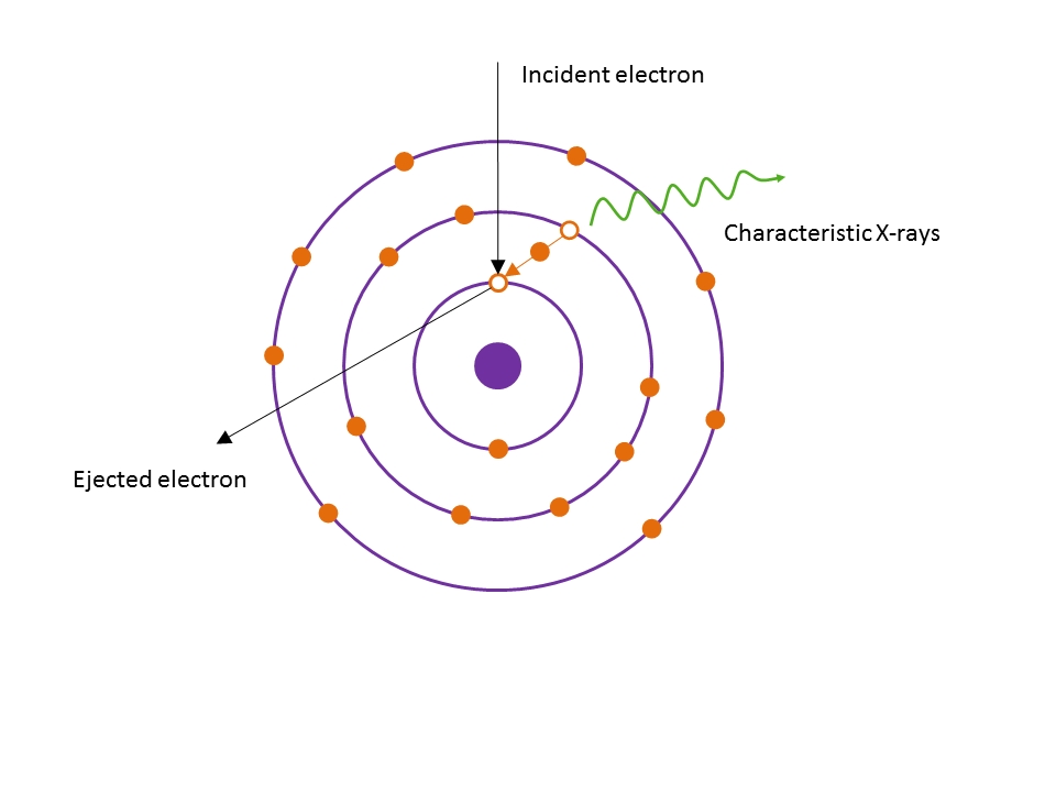
X-ray generation occurs as a result of the inelastic scattering processes after interaction between incident electrons and specimen. When a high energy electron of incident beam interacts with an atom within specimen, it results in the ejection of an electron from an inner atomic shell and the atom remains in an ionized or excited state with a vacancy in this shell. Subsequently, de-excitation takes place by moving an electron from an outer into the inner shell, which fills the vacancy. This action is accompanied with change in energy within the atom, unique to the element and called characteristic energy. This characteristic energy can be released from the atom by the emission of an X-ray photon with a specified energy to that transition and therefore, to the element. Schematic description of the characteristic X-ray formation EDS detectorApplication of the technique
The EDS analysis is usually used to analyse the chemical composition within the microstructure, which can help to define or identify:- different phases within the microstructure (for example: phases after casting, high temperature synthesis, annealing etc.)
- distribution of the elements within the cross-section (Element), lines, points, etc
- elemental mapping of surface (corrosion products, interface formation, solders, etc.).
Typical case studies
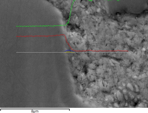
EDS point analysis of the Al2O3 / AlCa interface in aluminium matrix composites
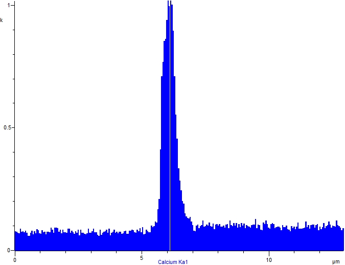
EDS line analysis: Distribution of the Ca at the Al2O3 / AlCa interface in aluminium matrix composites
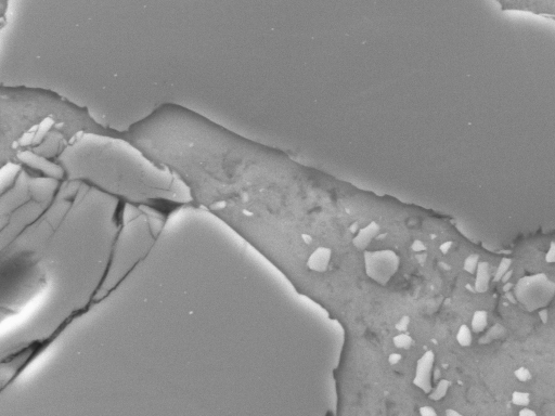
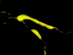
EDS elemental mapping: Distribution of the Ca at the Al2O3 / AlCa interface in aluminium matrix composites
Equipments
- JEOL 7600F Schotky field emission scanning electron microscope
- JEOL JSM 6610 Scanning electron microscope
- JEOL 5310-LV Scanning electron microscope
- Tescan VEGA3 XMU- Scanning electron microscope