Services / Material structure characterization /
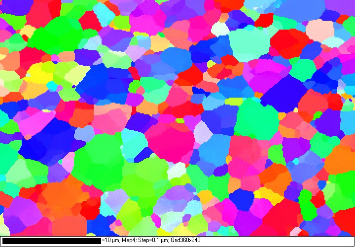 Inverse pole figure map
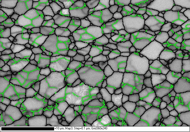 Band contrast map
Ľubomír Orovčík
Phase analysis
Electron backscatter diffraction analysis
General purpose
EBSD analysis is Scanning Electron Microscope based method which provides crystallographic information about the sample microstructure, on a millimetre to a micro or even nanometre scale.Basic crystallographic information which can be obtained via EBSD is focused to investigate a grain size or phase distribution, grain boundary characterization, texture and orientation of the crystals within the microstructure.Principle of operation
After anincident electron beam interacts with a tilted sample (crystalline), the diffracted electrons form a Kikuchi diffraction pattern (KDP), which is detected bythe fluorescent screen of the EBSD detector. The KDP is characteristic for the certain crystal structure and orientation in the sample region where it was generated. Usually,when electron beam scansthrough cross-section of the polycrystalline sample, the complete data set of crystal orientation at each point is collected in EBSD maps. Thus a complete and quantitative representation of the microstructure can be providedvia EBSD.Application of the technique
If SEM is equipped by EBSD detector, following information may be gathered from EBSD measurement:- study of the changes in grain size (for example: after heat treatment or severe plastic deformation techniques).
- study of the texture after forming operation or heat treatment.
- distribution of the various phases presented within microstructure.
- definition of the grain boundaries in terms of Low and High angle boundaries, special boundaries, twins etc.
Typical case studies
Inverse pole figure (IPF) map showing detail of the grain structure of the fine grained aluminium made from powders after extrusion and annealing and highlighted low (green) and high (black) angle grain boundaries in band contrast map Inverse pole figure map Band contrast mapEquipments
Contact
Martin NoskoĽubomír Orovčík